
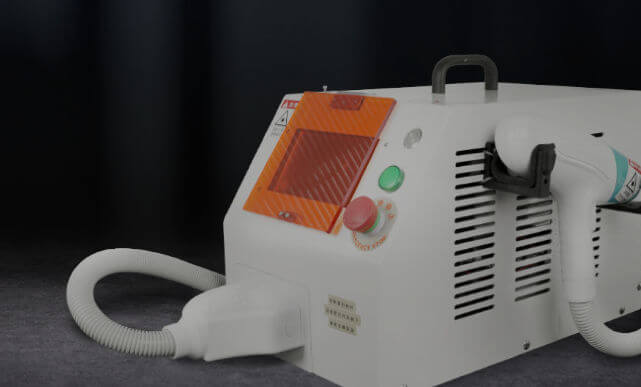
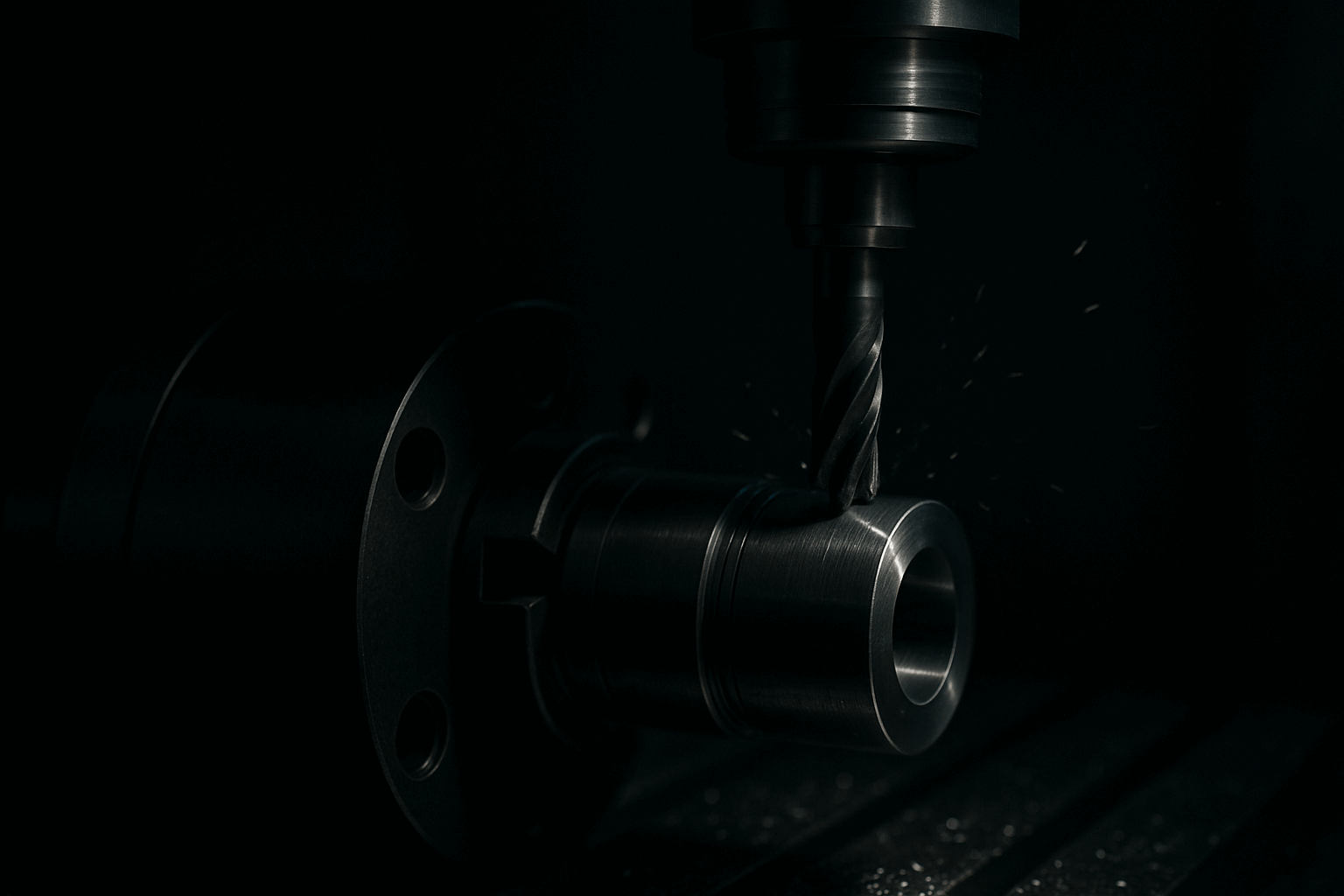
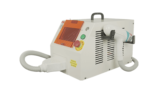
Laser Cleaner

Product Description
Advantages of Laser Cleaning in the Semiconductor Industry
- High-Precision Cleaning: Removes tiny contaminants (tin dross, photoresist residues, etc.) without damaging the substrate
- Non-Contact & No Consumables: Suitable for compact devices like smartphones
- Improves Yield Rate: Ensures conductivity and product stability
- Removes Micro Contaminants: Eliminates nano-scale particles and organic residues.
- Eco-Friendly & Cost-Effective: No chemical solvents, reducing pollution and disposal costs.
- Wide Application Range: Used for wafer, packaging, probe card, and PCB solder joint cleaning
- Precise Control: Adjustable laser parameters for optimal cleaning results Laser cleaning technology is widely used in semiconductor manufacturing due to its efficiency, precision, and eco-friendly nature, enhancing yield rate and process stability
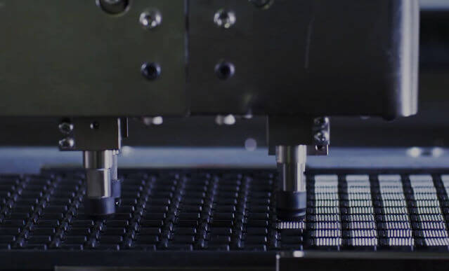
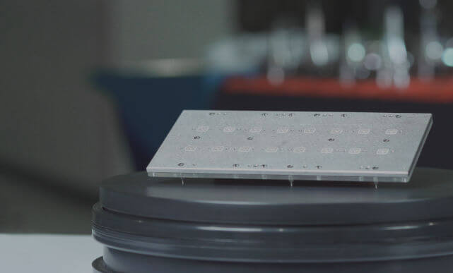
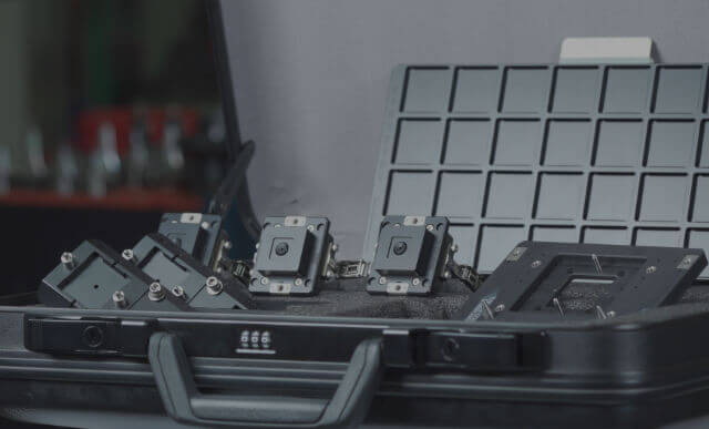
Laser Cleaner Use Cases in Semiconductor
-
Pogo Pin Cleaning
Before After 

-
Finger Pin Cleaning
Before After 

Product Specification
|
Max output power (1064nm)
|
When 1.5 Watts, corresponding to each energy is greater than 0.3 joules
|
|
Output power adjustment range (1064nm)
|
0.7 Watts to 1.5 Watts
|
|
Laser pulse width (1064nm)
|
below 50 ns (FWHM)
|
|
Operating temperature
|
between 15~40°C
|
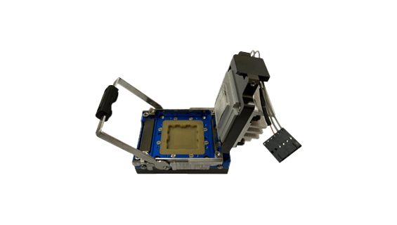
MORE PRODUCTS
-
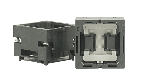
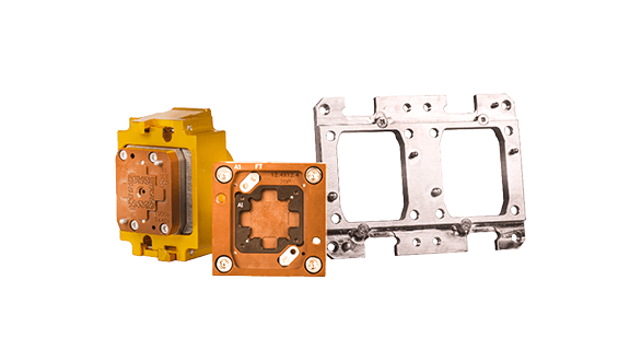 Package on Package Socket
-
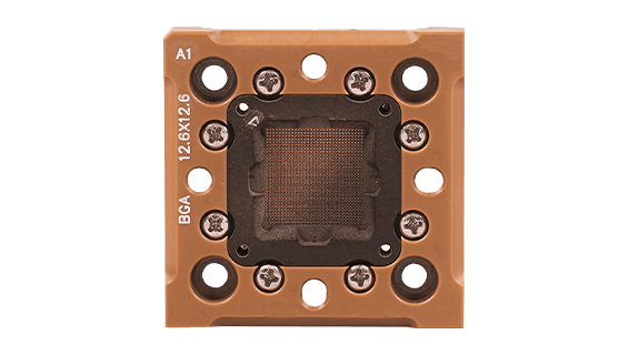
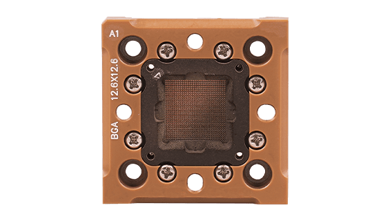 BGA Final Test Socket
-
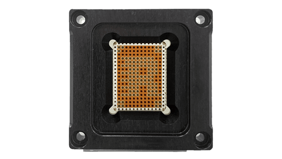
 QFN Final Test Socket
-
 Burn in Socket
-
 PCR Test Socket
-
 WLCSP Probe Heads
-
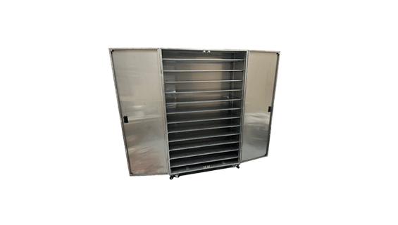
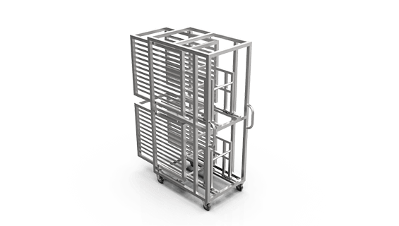 Semi-automatic Trolley for Burn-in Process
-
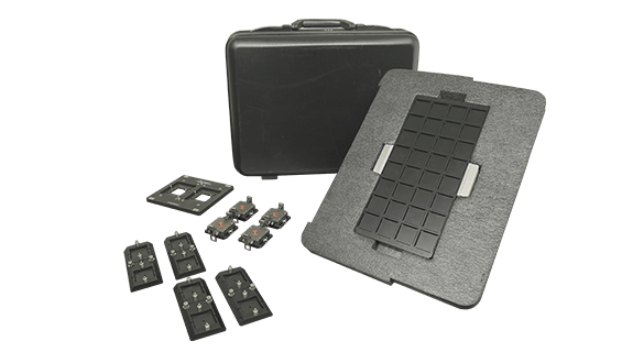 Handler Change Kit
-
 ESD Coating
-
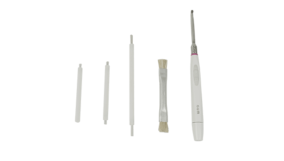 Socket Brush
-
 Clean Pad
-
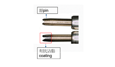 Non-stick Coating
-
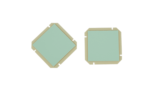
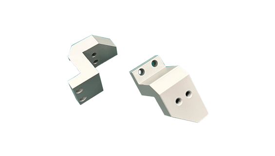
 Sheet Metal Processing
-
 CNC Precision Machining
-
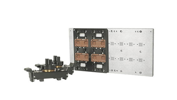
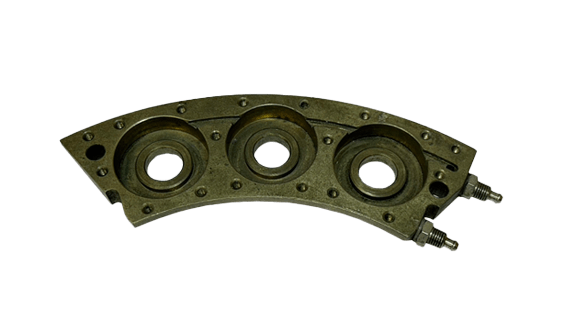
 Semiconductor Test Fixtures
-
 Automated Testing Sorter Components
Contact Us Now
Complete online forms and Pin-Jet will have representatives to help you with professional services
