
Understanding ESD: How It Damages Semiconductor Components and How to Prevent It
Electrostatic Discharge (ESD) is a phenomenon caused by the transfer of electric charge between two objects that are statically charged. This typically occurs when two objects with different electrical potentials come into contact or are brought close together, resulting in a rapid discharge of static electricity and a sudden flow of current.
ESD Damage: How Does It Affect Semiconductor Components?
Electrostatic Discharge (ESD) refers to the sudden release of electrical charge between two objects, which can significantly impact semiconductor components. Due to the miniature and precise internal structures of semiconductor devices, the high voltage and current from an ESD event can cause permanent damage, functional degradation, or even latent failures.
Common Types of ESD Failures
Electrostatic Discharge (ESD) can result in various types of failures, broadly categorized into immediate damage and latent damage. Below are the common types of ESD failures:
-
Thermal Damage:
High current generated during an ESD event creates extreme instantaneous heat within the component, causing metal layers to melt or break. -
Electrical Breakdown:
High voltage exceeds the breakdown voltage of internal insulation materials (such as oxide layers), leading to permanent damage to the insulation layer. -
Dielectric Layer Damage:
ESD causes structural damage or physical cracks in the dielectric layer of the component. -
Metal Melting or Arcing:
The large instantaneous current from ESD results in localized melting or arcing on metallic conductors. -
Transistor Damage:
ESD induces high voltage or high current within transistors, compromising their structural integrity. -
Logic Errors:
High-frequency pulses from ESD disrupt the operation of logic circuits within the component. -
Transient Failures:
ESD causes temporary functional interruptions without causing permanent structural damage to the component. -
Latent Damage:
Although ESD does not cause immediate failure, it leaves hidden defects within the component, potentially leading to future failures. -
Input/Output Interface Damage:
ESD directly damages the I/O interfaces of the component. -
Electromagnetic Interference (EMI) Failures:
High-frequency electromagnetic pulses generated by ESD interfere with the operation of surrounding components.
Common ESD Protection Techniques and Methods
-
Environmental Control Techniques:
*Increase air humidity
*Use anti-static flooring -
Equipment Protection Techniques:
*Grounding systems
*Static elimination devices -
Personal Protection Techniques:
*Anti-static wrist straps
*Anti-static footwear
*Anti-static clothing -
Design Protection Techniques:
*Protective components
*ESD protection capacitors
*Optimized circuit designs -
Packaging and Transportation Protection:
*Anti-static packaging
*Anti-static foam
*Anti-static containers -
Testing and Monitoring Techniques:
*Static charge monitoring
*Regular testing
ESD protection techniques integrate environmental control, equipment protection, personal protection, and design optimization. By implementing the above methods, the impact of ESD on semiconductor components and electronic devices can be significantly reduced, improving product quality and reliability while minimizing production losses and return rates.
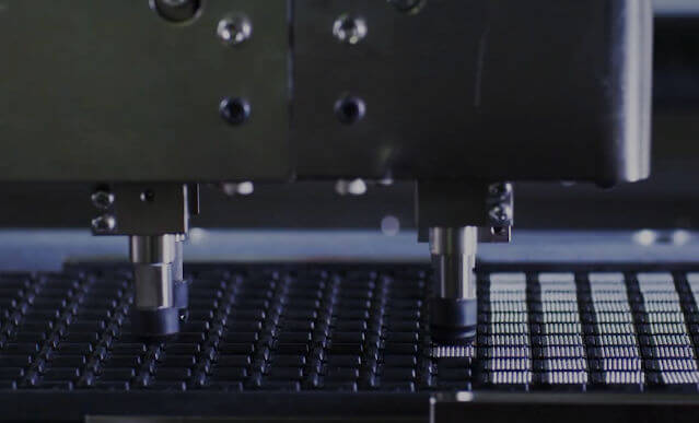
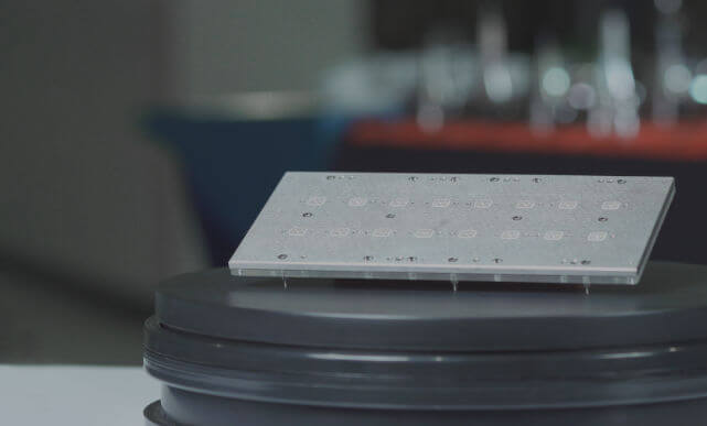
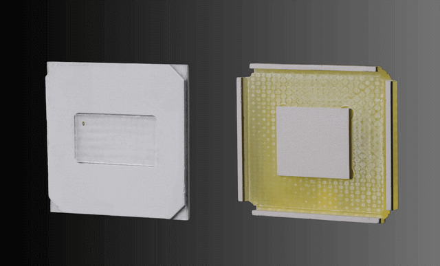
Introducing Pin-Jet's ESD Coating Technology
ESD Coating (Electrostatic Dissipative Coating) plays a critical role in preventing damage to components caused by electrostatic discharge (ESD).
-
Effective Prevention of ESD Damage: This coating effectively prevents ESD-induced damage to components, enhancing product reliability.
-
Superior Conductive Performance: The surface resistivity of the coating ranges from 1×10⁵Ω to 1×10⁹Ω, ensuring rapid dissipation of static electricity.
- Applicable to Various Testing Fixtures: Pin-Jet's ESD Coating can be applied to a wide range of testing fixtures, including IC test sockets, test boards, and more, meeting diverse customer requirements.
ESD Testing and Validation
ESD (Electrostatic Discharge) testing and validation aim to evaluate the resistance of electronic components or devices to electrostatic environments, ensuring their reliability in designed application scenarios.
-
Assessing Anti-Static Performance: Determine whether the product can withstand specific ESD conditions.
-
Validating Design Compliance: Ensure that the product meets industry standards (e.g., IEC, ANSI).
- Ensuring Reliability: Reduce product failures caused by electrostatic discharge.
Differences Between ESD and EOS
| Item | ESD (Electrostatic Discharge) | EOS (Electrical Overstress) |
|---|---|---|
| Definition | Sudden release of static electricity between two objects. | Prolonged exposure to excessive voltage, current, or power. |
| Duration | Very short (nanoseconds to microseconds). | Can last from milliseconds to seconds or longer. |
| Characteristics | High voltage and current spikes over a short duration. | Sustained stress, often causing overheating or damage. |
| Voltage/Current Nature | Rapid and intense voltage and current surges. | Continuous or sustained high voltage or current levels. |
| Impact Range | Localized damage to sensitive areas such as thin oxide layers. | Broader component damage, including overheating or burning. |
| Item | ESD Prevention | EOS Prevention |
| Environmental Control | Anti-static flooring, maintaining proper humidity. | Surge protectors, stable power supply systems. |
| Equipment Protection | Grounding systems, static eliminators. | Voltage/current limiters, proper circuit design. |
| Anti-static wrist straps, footwear, and clothing. | Training on proper handling of electrical devices. | |
| Design Optimization | ESD protection circuits, use of static dissipative materials. | Incorporation of over-voltage and over-current protection. |
-
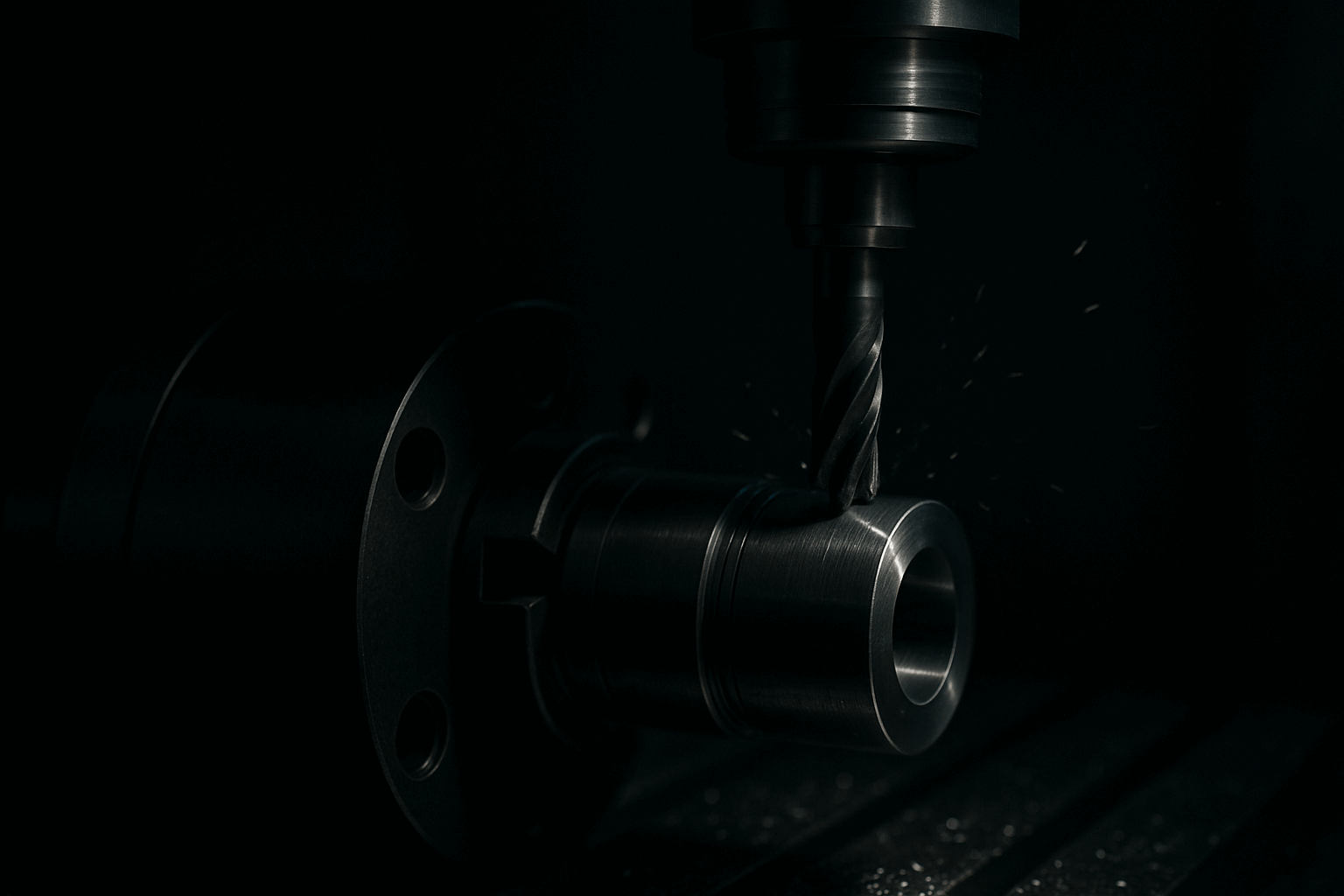
Head in Pillow Defect in BGA Soldering Process: Causes and Solutions
 2024.12.27
Head in Pillow Defect in BGA Soldering Process: Causes and Solutions
Head-in-Pillow (HIP) is a common failure mode in the BGA (Ball Grid Array) soldering process, referring to incomplete fusion between the BGA solder ball and the PCB pad, resulting in a structure resembling a "pillow and head." This defect can lead to poor contact, affecting the performance and reliability of electronic components.
2024.12.27
Head in Pillow Defect in BGA Soldering Process: Causes and Solutions
Head-in-Pillow (HIP) is a common failure mode in the BGA (Ball Grid Array) soldering process, referring to incomplete fusion between the BGA solder ball and the PCB pad, resulting in a structure resembling a "pillow and head." This defect can lead to poor contact, affecting the performance and reliability of electronic components.
-
Wafer Test Probe
 2024-12-23
Wafer Test Probe
Wafer Testing is an indispensable step in the semiconductor manufacturing process, responsible for inspecting the functionality and performance of each die on a wafer.
2024-12-23
Wafer Test Probe
Wafer Testing is an indispensable step in the semiconductor manufacturing process, responsible for inspecting the functionality and performance of each die on a wafer.
-
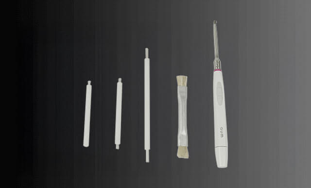
How to Clean Pogo Pins: Essential Tips for Effective Maintenance
 2024-12-20
How to Clean Pogo Pins: Essential Tips for Effective Maintenance
Pogo Pin is a commonly used spring-loaded probe in semiconductor testing equipment, designed to establish stable electrical connections with electronic components during the testing process. With frequent usage, Pogo Pins are prone to contamination (e.g., oxides, solder residues, or dust), which can result in poor contact and subsequently affect the accuracy and efficiency of testing.
2024-12-20
How to Clean Pogo Pins: Essential Tips for Effective Maintenance
Pogo Pin is a commonly used spring-loaded probe in semiconductor testing equipment, designed to establish stable electrical connections with electronic components during the testing process. With frequent usage, Pogo Pins are prone to contamination (e.g., oxides, solder residues, or dust), which can result in poor contact and subsequently affect the accuracy and efficiency of testing.
-
BGA (Ball Grid Array) Soldering Process: Defects and Solutions
2024-12-20
BGA (Ball Grid Array) Soldering Process: Defects and Solutions
The quality of solder balls in the BGA soldering process directly affects the performance and reliability of the product. Various defects, such as voids, bridging, misalignment, and cracks, may occur during the soldering process. These defects can result from factors like soldering materials, equipment parameters, process design, or storage conditions. By optimizing material selection, improving process parameters, and enhancing quality control, the occurrence of soldering defects can be significantly reduced, thereby improving product reliability and lifespan.
-
What is the Final Test in Semiconductor Manufacturing?
 2024-06-27
What is the Final Test in Semiconductor Manufacturing?
In the semiconductor manufacturing process, the Final Test (FT) is a critical step that ensures each chip meets the expected performance standards before being shipped.
2024-06-27
What is the Final Test in Semiconductor Manufacturing?
In the semiconductor manufacturing process, the Final Test (FT) is a critical step that ensures each chip meets the expected performance standards before being shipped.
-
What is a QFN Socket? Key Benefits and Uses
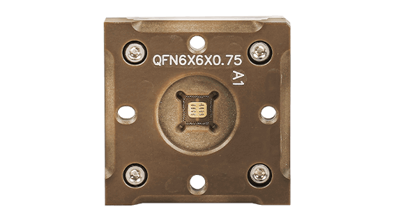 2024-06-12
What is a QFN Socket? Key Benefits and Uses
QFN Socket (Quad Flat No-lead) is a type of leadless surface-mount package used for integrated circuits.
2024-06-12
What is a QFN Socket? Key Benefits and Uses
QFN Socket (Quad Flat No-lead) is a type of leadless surface-mount package used for integrated circuits.
-
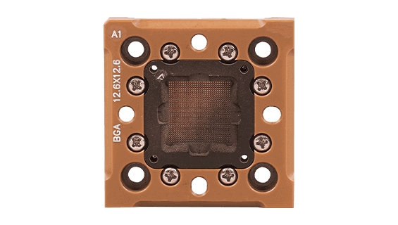
BGA Sockets Basics: Exploring Benefits and Application
 2024-06-05
BGA Sockets Basics: Exploring Benefits and Application
A BGA socket (Ball Grid Array socket) is a type of surface mount packaging used for integrated circuits.
2024-06-05
BGA Sockets Basics: Exploring Benefits and Application
A BGA socket (Ball Grid Array socket) is a type of surface mount packaging used for integrated circuits.
-
Test Sockets: Key Components in IC Testing
2024-05-29
Test Sockets: Key Components in IC Testing
This article will explore why Test Sockets are important, the different kinds there are, and how they are used in the semiconductor industry.
Contact Us Now
Complete online forms and Pin-Jet will have representatives to help you with professional services