

2024.12.27
Blog
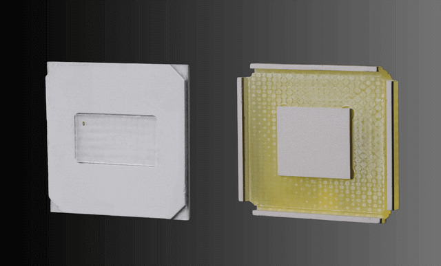
Head in Pillow Defect in BGA Soldering Process: Causes and Solutions
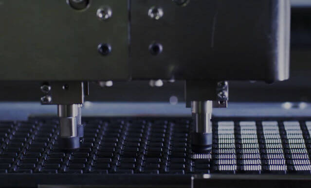
Head-in-Pillow (HIP) is a common failure mode in the BGA (Ball Grid Array) soldering process, referring to incomplete fusion between the BGA solder ball and the PCB pad, resulting in a structure resembling a "pillow and head." This bga soldering defect can lead to poor contact, affecting the performance and reliability of electronic components. Below is a detailed analysis of common failure issues and solutions related to the HIP phenomenon:
1. Incomplete Reflow
-
Issue Description:
Clean Pad is a tool specifically designed for cleaning Pogo Pins, effectively removing surface contaminants without damaging the probes.The solder ball does not fully melt, failing to form a strong connection with the PCB pad. This can result in intermittent contact issues or signal instability during testing.
-
Solutions:
A. Use an anti-static brush to remove surface dust and debris.A. Adjust Reflow Profile:
Ensure the reflow soldering temperature profile matches the solder alloy's melting requirements. Extend the soak time as needed to allow the solder balls to fully melt.
B. Inspect Solder Paste Application:
Verify the solder paste's printing thickness is uniform to avoid insufficient paste, which could reduce the contact area.
C. Optimize Equipment Parameters:
Use X-ray or microscopic inspection to check the solder joints after reflow to confirm proper soldering.
to ensure it has regained good contact performance.
2. Oxidation-Induced Soldering Failures
-
Issue Description:
An oxidation layer forms after soldering, preventing full bonding between the solder ball and the PCB pad. This reduces the mechanical strength and conductivity of the solder joints.
-
Solutions:
A. Control Material Quality:
Use fresh, non-oxidized BGA solder balls and solder paste, avoiding components that have been stored for long periods.
B. Enhance Flux Performance:
Select solder paste with a flux that has stronger deoxidation capabilities, suitable for high-reliability soldering requirements.
C. Improve Storage Conditions:
Store BGA components in low-humidity, oxidation-free environments to minimize the formation of oxidation layers.
3. Stencil Misalignment
-
Issue Description:
Solder paste is not correctly applied to the pads, leading to misaligned solder balls or incomplete contact with the pads after reflow soldering.
-
Solutions:
A. Calibrate Printing Equipment:
Regularly calibrate printing equipment to ensure the solder paste is aligned accurately with the pads. B. Select Appropriate Stencils:
Ensure the stencil aperture size and thickness meet design specifications to prevent solder paste misalignment.
C. Inspect Printing Quality:
Use Automatic Optical Inspection (AOI) systems to check the quality of solder paste application.
4. Solder Joint Stress
-
Issue Description:
Cracks or joint delamination occur due to stress during the cooling process after soldering.
-
Solutions:
A. Optimize Cooling Process:
Adjust the cooling curve after reflow soldering to minimize stress caused by rapid temperature changes.
B. Select Suitable Materials:
Use PCB materials with a thermal expansion coefficient that matches the components to reduce stress accumulation during cooling.
C. Strengthen Solder Joint Mechanics:
Increase the solder paste thickness or optimize soldering parameters to enhance the mechanical strength of the solder joints.
5. Solder Paste Quality Issues
-
Issue Description:
Bubbles or impurities in the solder paste can result in voids or delamination within the solder joints after reflow soldering.
-
Solutions:
A. Use High-Quality Solder Paste:
Choose high-reliability solder paste that meets process requirements and avoid using expired or poorly stored products.
B. Enhance Solder Paste Preparation:
Thoroughly stir the solder paste before use to ensure uniform mixing.
C. Check Solder Paste Storage Conditions:
Store solder paste under appropriate temperature and humidity conditions to prevent moisture absorption or contamination.
6. PCB Pad Issues
-
Issue Description:
Contamination or unevenness on the PCB pad surface leads to poor contact between the solder ball and the pad.
-
Solutions:
A. Clean the Pad Surface:
Use professional cleaning agents to remove contaminants from the pad surface, ensuring it is clean and flat.
B. Inspect Pad Coating:
Verify that the thickness and material of the pad coating meet design specifications, avoiding excessively thick oxide layers.
C. Optimize PCB Manufacturing Process:
Collaborate with PCB suppliers to improve pad manufacturing processes and enhance surface quality.
Related News
-
Understanding ESD: How It Damages Semiconductor Components and How to Prevent It
 2024-12-23
Understanding ESD: How It Damages Semiconductor Components and How to Prevent It
Electrostatic Discharge (ESD) is a phenomenon caused by the transfer of electric charge between two objects that are statically charged. This typically occurs when two objects with different electrical potentials come into contact or are brought close together, resulting in a rapid discharge of static electricity and a sudden flow of current.
2024-12-23
Understanding ESD: How It Damages Semiconductor Components and How to Prevent It
Electrostatic Discharge (ESD) is a phenomenon caused by the transfer of electric charge between two objects that are statically charged. This typically occurs when two objects with different electrical potentials come into contact or are brought close together, resulting in a rapid discharge of static electricity and a sudden flow of current.
-
Wafer Test Probe
 2024-12-23
Wafer Test Probe
Wafer Testing is an indispensable step in the semiconductor manufacturing process, responsible for inspecting the functionality and performance of each die on a wafer.
2024-12-23
Wafer Test Probe
Wafer Testing is an indispensable step in the semiconductor manufacturing process, responsible for inspecting the functionality and performance of each die on a wafer.
-
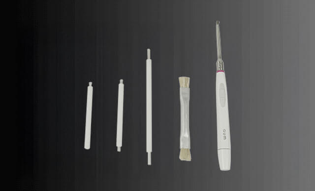
How to Clean Pogo Pins: Essential Tips for Effective Maintenance
2024-12-20
How to Clean Pogo Pins: Essential Tips for Effective Maintenance
Pogo Pin is a commonly used spring-loaded probe in semiconductor testing equipment, designed to establish stable electrical connections with electronic components during the testing process. With frequent usage, Pogo Pins are prone to contamination (e.g., oxides, solder residues, or dust), which can result in poor contact and subsequently affect the accuracy and efficiency of testing.
-
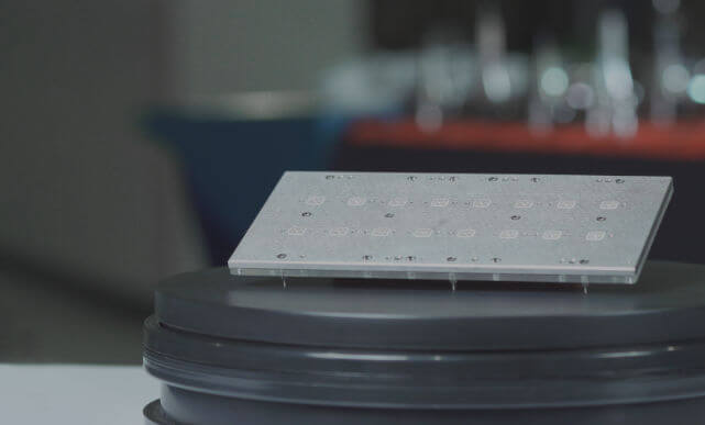
BGA (Ball Grid Array) Soldering Process: Defects and Solutions
2024-12-20
BGA (Ball Grid Array) Soldering Process: Defects and Solutions
The quality of solder balls in the BGA soldering process directly affects the performance and reliability of the product. Various defects, such as voids, bridging, misalignment, and cracks, may occur during the soldering process. These defects can result from factors like soldering materials, equipment parameters, process design, or storage conditions. By optimizing material selection, improving process parameters, and enhancing quality control, the occurrence of soldering defects can be significantly reduced, thereby improving product reliability and lifespan.
-
What is the Final Test in Semiconductor Manufacturing?
 2024-06-27
What is the Final Test in Semiconductor Manufacturing?
In the semiconductor manufacturing process, the Final Test (FT) is a critical step that ensures each chip meets the expected performance standards before being shipped.
2024-06-27
What is the Final Test in Semiconductor Manufacturing?
In the semiconductor manufacturing process, the Final Test (FT) is a critical step that ensures each chip meets the expected performance standards before being shipped.
-
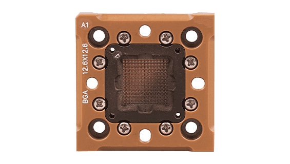
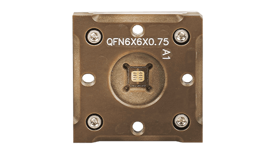
What is a QFN Socket? Key Benefits and Uses
 2024-06-12
What is a QFN Socket? Key Benefits and Uses
QFN Socket (Quad Flat No-lead) is a type of leadless surface-mount package used for integrated circuits.
2024-06-12
What is a QFN Socket? Key Benefits and Uses
QFN Socket (Quad Flat No-lead) is a type of leadless surface-mount package used for integrated circuits.
-
BGA Sockets Basics: Exploring Benefits and Application
 2024-06-05
BGA Sockets Basics: Exploring Benefits and Application
A BGA socket (Ball Grid Array socket) is a type of surface mount packaging used for integrated circuits.
2024-06-05
BGA Sockets Basics: Exploring Benefits and Application
A BGA socket (Ball Grid Array socket) is a type of surface mount packaging used for integrated circuits.
-
Test Sockets: Key Components in IC Testing
2024-05-29
Test Sockets: Key Components in IC Testing
This article will explore why Test Sockets are important, the different kinds there are, and how they are used in the semiconductor industry.
Contact Us Now
Complete online forms and Pin-Jet will have representatives to help you with professional services