
What is the Final Test in Semiconductor Manufacturing?
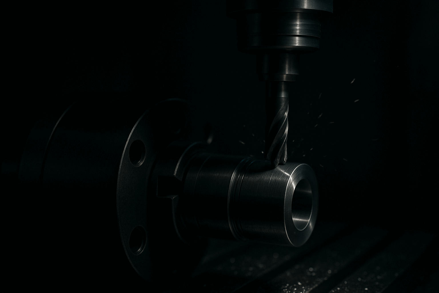
In the semiconductor manufacturing process, the Final Test (FT) is a critical step that ensures each chip meets the expected performance standards before being shipped. This testing phase involves comprehensive functional and performance tests on the chips to verify their reliability and efficacy in real-world applications.
The final test is usually conducted after the chips have been packaged, with testing equipment conducting electrical tests through the pins on the chip. This includes assessing various aspects such as power consumption, frequency, and I/O functionalities. Through these tests, chips that exhibit manufacturing defects or subpar performance can be identified and eliminated.
The final test not only enhances the overall quality of the product but also safeguards the interests of consumers and semiconductor companies, preventing costs and reputational damage associated with product failures. As technology advances, the techniques used in final testing continually evolve to address the increasingly complex chip designs and higher performance demands.
Detailed Explanation of the Semiconductor Final Test Process
The final testing process in semiconductors is a critical step to ensure that chips meet functionality, reliability, and quality requirements before leaving the factory. This process aims to identify and segregate conforming products, eliminate defective units, and categorize chips to meet diverse market demands.
Below is a summary of the semiconductor final testing process:
- Product Receiving and Inspection
- Electrical and Functional Testing
- Burn-In Testing (Optional)
- Environmental Stress Testing (Optional)
- Sorting and Grading
- Final Inspection
-
Packaging and Shipment
| Feature | Wafer Test | Final Test |
|---|---|---|
| Definition | Testing is conducted on each die on the wafer after wafer fabrication is complete to verify functionality. | Comprehensive testing is conducted on completed products after packaging to ensure conformity and customer satisfaction. |
| Testing Phase | Post-wafer fabrication, pre-packaging | Post-packaging |
| Testing Objectives | -Identify defective dies in the early stage, reducing processing waste. | -Verify the functionality and performance of packaged products. |
| - Provide initial test data for wafers to support yield and degradation analysis. | - Ensure the final product meets design specifications for integrity and reliability. | |
| Testing Subjects | Individual die | Packaged chips |
| Testing Equipment | Probe station and probe card | IC Test sockets and testing systems |
| Testing Contents | Basic functional and parameter testing | Functional, performance, reliability, and application scenario testing |
| Testing Results | Marking defective dies and generating a wafer map | Sorting, grading, and preparation for shipment. |
Wafer Sort vs Final Test
Wafer testing focuses on early-stage screening during the wafer fabrication process, effectively minimizing resource waste in the packaging phase.
Chip testing, on the other hand, is critical for ensuring the quality of the final product, encompassing more comprehensive performance and reliability testing.
These two testing stages complement each other, ensuring high efficiency and superior quality throughout the semiconductor manufacturing process.
-
Head in Pillow Defect in BGA Soldering Process: Causes and Solutions
 2024.12.27
Head in Pillow Defect in BGA Soldering Process: Causes and Solutions
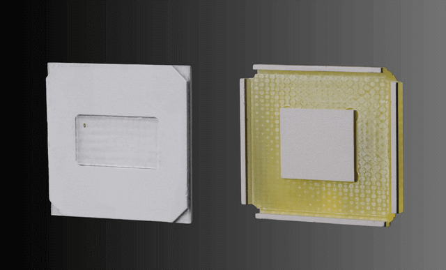
Head-in-Pillow (HIP) is a common failure mode in the BGA (Ball Grid Array) soldering process, referring to incomplete fusion between the BGA solder ball and the PCB pad, resulting in a structure resembling a "pillow and head." This defect can lead to poor contact, affecting the performance and reliability of electronic components.
2024.12.27
Head in Pillow Defect in BGA Soldering Process: Causes and Solutions
Head-in-Pillow (HIP) is a common failure mode in the BGA (Ball Grid Array) soldering process, referring to incomplete fusion between the BGA solder ball and the PCB pad, resulting in a structure resembling a "pillow and head." This defect can lead to poor contact, affecting the performance and reliability of electronic components.
-
Understanding ESD: How It Damages Semiconductor Components and How to Prevent It
 2024-12-23
Understanding ESD: How It Damages Semiconductor Components and How to Prevent It
Electrostatic Discharge (ESD) is a phenomenon caused by the transfer of electric charge between two objects that are statically charged. This typically occurs when two objects with different electrical potentials come into contact or are brought close together, resulting in a rapid discharge of static electricity and a sudden flow of current.
2024-12-23
Understanding ESD: How It Damages Semiconductor Components and How to Prevent It
Electrostatic Discharge (ESD) is a phenomenon caused by the transfer of electric charge between two objects that are statically charged. This typically occurs when two objects with different electrical potentials come into contact or are brought close together, resulting in a rapid discharge of static electricity and a sudden flow of current.
-
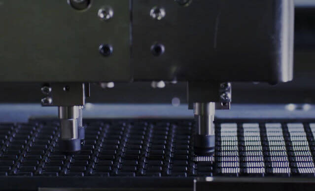
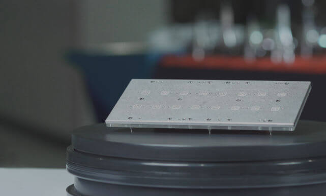
Wafer Test Probe
 2024-12-23
Wafer Test Probe
Wafer Testing is an indispensable step in the semiconductor manufacturing process, responsible for inspecting the functionality and performance of each die on a wafer.
2024-12-23
Wafer Test Probe
Wafer Testing is an indispensable step in the semiconductor manufacturing process, responsible for inspecting the functionality and performance of each die on a wafer.
-
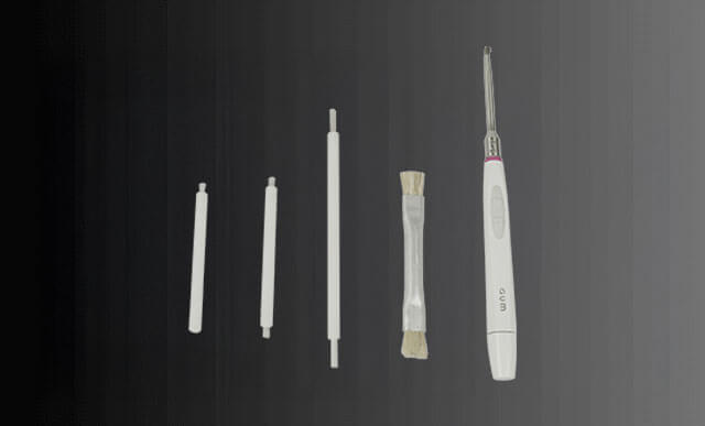
How to Clean Pogo Pins: Essential Tips for Effective Maintenance
2024-12-20
How to Clean Pogo Pins: Essential Tips for Effective Maintenance
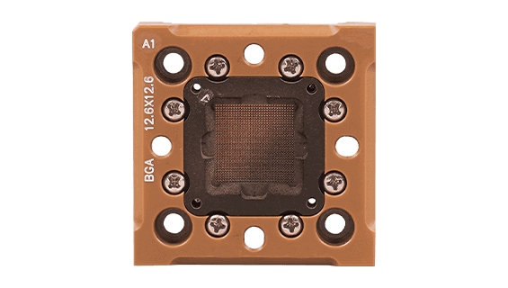
Pogo Pin is a commonly used spring-loaded probe in semiconductor testing equipment, designed to establish stable electrical connections with electronic components during the testing process. With frequent usage, Pogo Pins are prone to contamination (e.g., oxides, solder residues, or dust), which can result in poor contact and subsequently affect the accuracy and efficiency of testing.
-
BGA (Ball Grid Array) Soldering Process: Defects and Solutions
2024-12-20
BGA (Ball Grid Array) Soldering Process: Defects and Solutions
The quality of solder balls in the BGA soldering process directly affects the performance and reliability of the product. Various defects, such as voids, bridging, misalignment, and cracks, may occur during the soldering process. These defects can result from factors like soldering materials, equipment parameters, process design, or storage conditions. By optimizing material selection, improving process parameters, and enhancing quality control, the occurrence of soldering defects can be significantly reduced, thereby improving product reliability and lifespan.
-
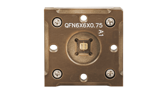
What is a QFN Socket? Key Benefits and Uses
 2024-06-12
What is a QFN Socket? Key Benefits and Uses
QFN Socket (Quad Flat No-lead) is a type of leadless surface-mount package used for integrated circuits.
2024-06-12
What is a QFN Socket? Key Benefits and Uses
QFN Socket (Quad Flat No-lead) is a type of leadless surface-mount package used for integrated circuits.
-
BGA Sockets Basics: Exploring Benefits and Application
 2024-06-05
BGA Sockets Basics: Exploring Benefits and Application
A BGA socket (Ball Grid Array socket) is a type of surface mount packaging used for integrated circuits.
2024-06-05
BGA Sockets Basics: Exploring Benefits and Application
A BGA socket (Ball Grid Array socket) is a type of surface mount packaging used for integrated circuits.
-
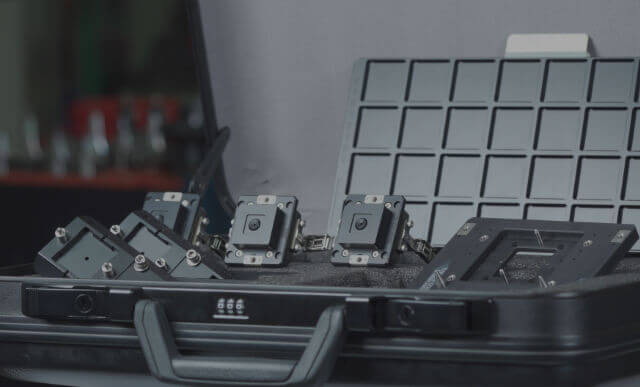
Test Sockets: Key Components in IC Testing
2024-05-29
Test Sockets: Key Components in IC Testing
This article will explore why Test Sockets are important, the different kinds there are, and how they are used in the semiconductor industry.
Contact Us Now
Complete online forms and Pin-Jet will have representatives to help you with professional services