
BGA Sockets Basics: Exploring Benefits and Application
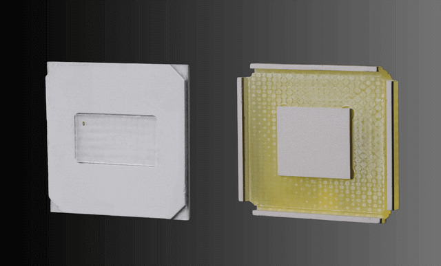
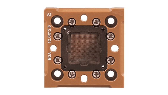
A BGA socket (Ball Grid Array socket) is a type of surface mount packaging used for integrated circuits. Unlike other packaging methods such as Pin Grid Array (PGA) or Dual In-line Package (DIP), a BGA socket uses an array of tiny solder balls on the underside of the chip to create electrical connections.
Here are some key features and advantages of BGA sockets :
- High Density: BGA sockets allow for high-density connections, making this packaging technology suitable for modern high-performance chips that require numerous connections to function properly.
- Performance Enhancement : The short leads of BGA sockets reduce inductance and resistance, thus improving electrical performance and signal transmission speed.
- Thermal Management : Compared to other types of packaging, BGA sockets offer better heat dissipation capabilities. The solder balls can more effectively transfer heat away from the chip.
- Reliability : Using solder balls instead of pins reduces the risk of damage during installation and handling, enhancing the reliability of the connections.
- Automated Assembly: BGA sockets are well-suited for automated assembly processes, making them commonly used in the mass production of electronic devices.
BGA sockets are widely used in microprocessors, GPUs, FPGAs, and other high-performance integrated circuits. They are commonly found in consumer electronics, telecommunications equipment, and computing devices.
Test sockets play a crucial role in the production process by ensuring the reliability and functionality of BGA components before final assembly. They allow for thorough testing and validation, reducing the risk of defects and enhancing overall product quality. If you’re interested in learning more about our BGA test sockets and how they can improve your production efficiency, please contact us for more information. Our team is here to assist you with all your testing needs.
-
Head in Pillow Defect in BGA Soldering Process: Causes and Solutions
 2024.12.27
Head in Pillow Defect in BGA Soldering Process: Causes and Solutions
Head-in-Pillow (HIP) is a common failure mode in the BGA (Ball Grid Array) soldering process, referring to incomplete fusion between the BGA solder ball and the PCB pad, resulting in a structure resembling a "pillow and head." This defect can lead to poor contact, affecting the performance and reliability of electronic components.
2024.12.27
Head in Pillow Defect in BGA Soldering Process: Causes and Solutions
Head-in-Pillow (HIP) is a common failure mode in the BGA (Ball Grid Array) soldering process, referring to incomplete fusion between the BGA solder ball and the PCB pad, resulting in a structure resembling a "pillow and head." This defect can lead to poor contact, affecting the performance and reliability of electronic components.
-
Understanding ESD: How It Damages Semiconductor Components and How to Prevent It
 2024-12-23
Understanding ESD: How It Damages Semiconductor Components and How to Prevent It
Electrostatic Discharge (ESD) is a phenomenon caused by the transfer of electric charge between two objects that are statically charged. This typically occurs when two objects with different electrical potentials come into contact or are brought close together, resulting in a rapid discharge of static electricity and a sudden flow of current.
2024-12-23
Understanding ESD: How It Damages Semiconductor Components and How to Prevent It
Electrostatic Discharge (ESD) is a phenomenon caused by the transfer of electric charge between two objects that are statically charged. This typically occurs when two objects with different electrical potentials come into contact or are brought close together, resulting in a rapid discharge of static electricity and a sudden flow of current.
-
Wafer Test Probe
 2024-12-23
Wafer Test Probe
Wafer Testing is an indispensable step in the semiconductor manufacturing process, responsible for inspecting the functionality and performance of each die on a wafer.
2024-12-23
Wafer Test Probe
Wafer Testing is an indispensable step in the semiconductor manufacturing process, responsible for inspecting the functionality and performance of each die on a wafer.
-
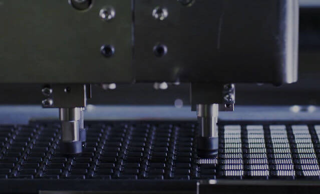
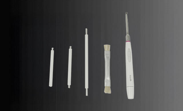
How to Clean Pogo Pins: Essential Tips for Effective Maintenance
2024-12-20
How to Clean Pogo Pins: Essential Tips for Effective Maintenance
Pogo Pin is a commonly used spring-loaded probe in semiconductor testing equipment, designed to establish stable electrical connections with electronic components during the testing process. With frequent usage, Pogo Pins are prone to contamination (e.g., oxides, solder residues, or dust), which can result in poor contact and subsequently affect the accuracy and efficiency of testing.
-
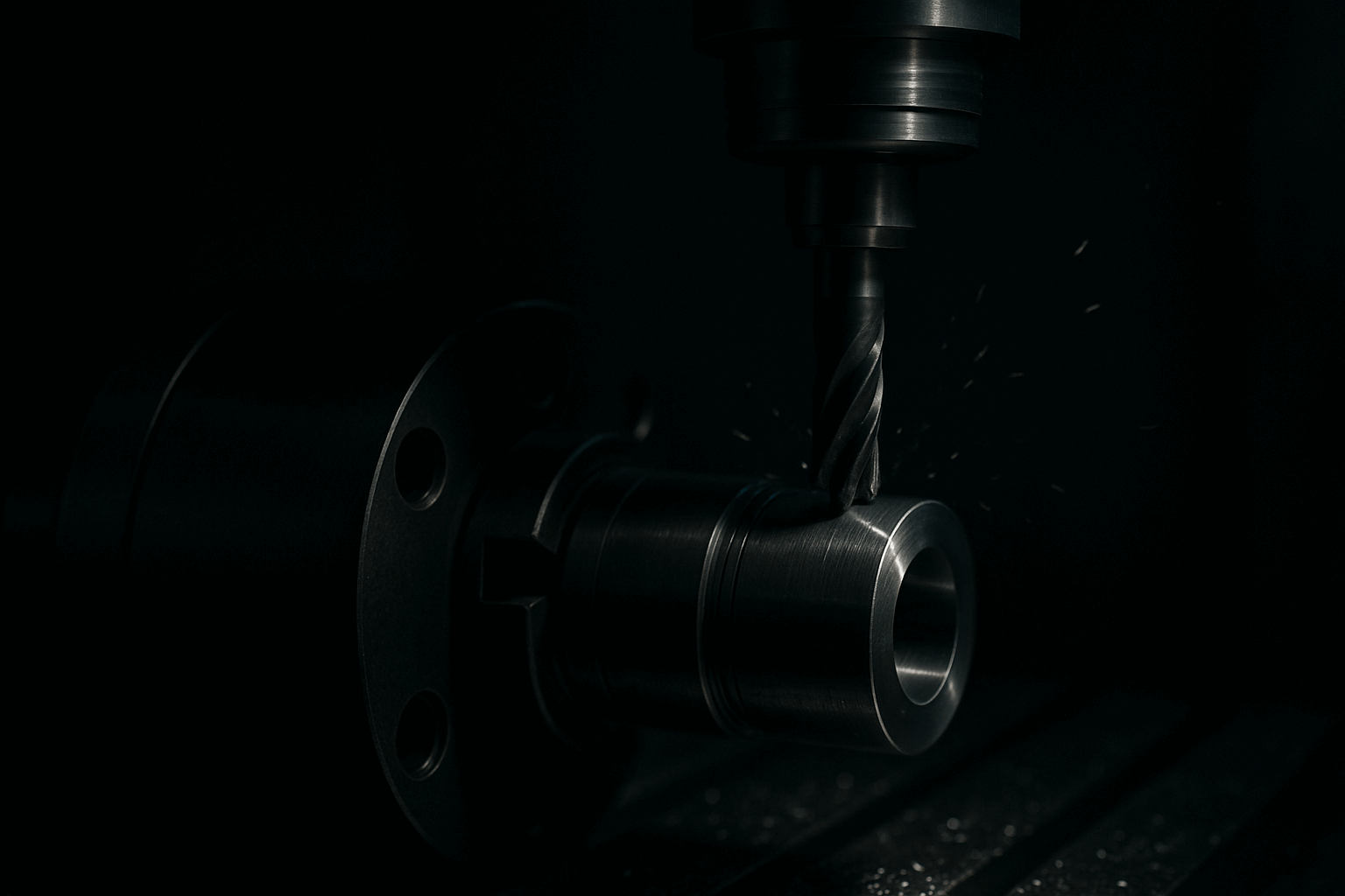
BGA (Ball Grid Array) Soldering Process: Defects and Solutions
2024-12-20
BGA (Ball Grid Array) Soldering Process: Defects and Solutions
The quality of solder balls in the BGA soldering process directly affects the performance and reliability of the product. Various defects, such as voids, bridging, misalignment, and cracks, may occur during the soldering process. These defects can result from factors like soldering materials, equipment parameters, process design, or storage conditions. By optimizing material selection, improving process parameters, and enhancing quality control, the occurrence of soldering defects can be significantly reduced, thereby improving product reliability and lifespan.
-
What is the Final Test in Semiconductor Manufacturing?
 2024-06-27
What is the Final Test in Semiconductor Manufacturing?
In the semiconductor manufacturing process, the Final Test (FT) is a critical step that ensures each chip meets the expected performance standards before being shipped.
2024-06-27
What is the Final Test in Semiconductor Manufacturing?
In the semiconductor manufacturing process, the Final Test (FT) is a critical step that ensures each chip meets the expected performance standards before being shipped.
-
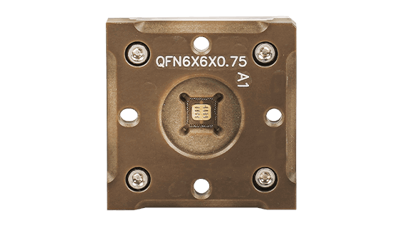
What is a QFN Socket? Key Benefits and Uses
 2024-06-12
What is a QFN Socket? Key Benefits and Uses
QFN Socket (Quad Flat No-lead) is a type of leadless surface-mount package used for integrated circuits.
2024-06-12
What is a QFN Socket? Key Benefits and Uses
QFN Socket (Quad Flat No-lead) is a type of leadless surface-mount package used for integrated circuits.
-
Test Sockets: Key Components in IC Testing
 2024-05-29
Test Sockets: Key Components in IC Testing
This article will explore why Test Sockets are important, the different kinds there are, and how they are used in the semiconductor industry.
2024-05-29
Test Sockets: Key Components in IC Testing
This article will explore why Test Sockets are important, the different kinds there are, and how they are used in the semiconductor industry.
Contact Us Now
Complete online forms and Pin-Jet will have representatives to help you with professional services